Gallium(III) oxide – Wikipedia
From Wikipedia, the free encyclopedia
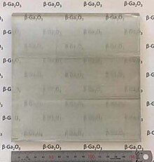
β-Ga2O3 crystal |
|
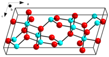
Crystal structure of β-Ga2O3 |
|
| Names | |
|---|---|
| Other names
gallium trioxide, gallium sesquioxide |
|
| Identifiers | |
| ChemSpider | |
| ECHA InfoCard | 100.031.525 |
| EC Number | |
| RTECS number | |
| UNII | |
|
|
| Properties | |
| Ga2O3 | |
| Molar mass | 187.444 g/mol[1] |
| Appearance | white crystalline powder |
| Density | α-phase: 6.44 g/cm3 β-phase: 5.88 g/cm3 |
| Melting point | 1,900 °C (3,450 °F; 2,170 K) alpha 1725 °C, beta [2] |
| insoluble | |
| Solubility | soluble in most acids |
| Band gap | α-phase: 5.3-5.4 eV β-phase: 4.7-4.9 eV |
| Structure | |
| α: Trigonal, hR30, space group = R3c, No. 167[3]
β: Monoclinic, mS20, space group = C2/m, No. 12[4] |
|
|
a = 0.49825 / 1.2232 nm, b = 0.49825 / 0.3041 nm, c = 1.3433 / 0.5801 nm α = 90 / 90°, β = 90 / 103.73°, γ = 120 / 90°[5] / [6]
α-phase / β-phase |
|
| 6 / 4 | |
| Thermochemistry | |
| 92.1 J/mol·K[7] | |
| 85.0 J/mol·K[7] | |
| −1089.1 kJ/mol[7] | |
| -998.3 kJ/mol[7] | |
|
Except where otherwise noted, data are given for materials in their standard state (at 25 °C [77 °F], 100 kPa).
|
|
Chemical compound
Gallium(III) oxide is an inorganic compound and ultra-wide bandgap semiconductor with the formula Ga2O3. It is actively studied for applications in power electronics, phosphors, and gas sensing.[8][9][10] The compound has several polymorphs, of which the monoclinic β-phase is the most stable. The β-phase’s bandgap of 4.7–4.9 eV and large-area, native substrates make it a promising competitor to GaN and SiC-based power electronics applications and solar-blind UV photodetectors.[10][11] Ga2O3 exhibits reduced thermal conductivity and electron mobility by an order of magnitude compared to GaN and SiC, but is predicted to be significantly more cost-effective due to being the only wide-bandgap material capable of being grown from melt.[10][12][13] β-Ga2O3 is thought to be radiation hard which makes it promising for military and space applications.[14][15]
Preparation[edit]
Gallium trioxide is precipitated in hydrated form upon neutralization of acidic or basic solution of gallium salt. Also, it is formed on heating gallium in air or by thermally decomposing gallium nitrate at 200–250 ˚C.
Crystalline Ga2O3 can occur in five polymorphs, α, β, γ, δ, and ε. Of these polymorphs β-Ga2O3 is the most thermodynamically stable phase at standard temperature and pressure[16] while α-Ga2O3 is the most stable polymorph under high pressures.[17]
Bulk substrates of β-Ga2O3 can be produced, which is one of the major advantages of this material system. Bulk substrates can be produced in multiple orientations and by multiple techniques.[23][24]

- α-Ga2O3 can be obtained by heating β-Ga2O3 at 65 kbars and 1100 °C. It has a corundum structure. The hydrated form can be prepared by decomposing precipitated and “aged” gallium hydroxide at 500 °C. Epitaxial thin films of α-Ga2O3 deposited on c-plane (0001), m-plane (10-10), or a-plane (11-20) sapphire substrates have been demonstrated.
- γ-Ga2O3 is prepared by rapidly heating the hydroxide gel at 400–500 °C. A more crystalline form of this polymorph can be prepared directly from gallium metal by a solvothermal synthesis.[25]
- δ-Ga2O3 is obtained by heating Ga(NO3)3 at 250 °C.[26]
- ε-Ga2O3 is prepared by heating δ-Ga2O3 at 550 °C.[16] Thin films of ε-Ga2O3 are deposited by means of metalorganic vapour-phase epitaxy using trimethylgallium and water on sapphire substrates at temperatures between 550 and 650 °C [27]
Reactions[edit]
Gallium(III) trioxide is amphoteric.[28] It reacts with alkali metal oxides at high temperature to form, e.g., NaGaO2, and with Mg, Zn, Co, Ni, Cu oxides to form spinels, e.g., MgGa2O4.[29]
It dissolves in strong alkali to form a solution of the gallate ion, Ga(OH)−
4.
With HCl, it forms gallium trichloride GaCl3.[30]
- Ga2O3 + 6 HCl → 2 GaCl3 + 3 H2O
It can be reduced to gallium suboxide (gallium(I) oxide) Ga2O by H2.[31] or by reaction with gallium metal:[32]
- Ga2O3 + 2 H2 → Ga2O + 2 H2O
- Ga2O3 + 4 Ga → 3 Ga2O
Structure[edit]
β-Ga2O3, with a melting point of 1900 ˚C, is the most stable crystalline modification. The oxide ions are in a distorted cubic closest packing arrangement, and the gallium (III) ions occupy distorted tetrahedral and octahedral sites, with Ga–O bond distances of 1.83 and 2.00 Å respectively.[33]
α-Ga2O3 has the same structure (corundum) as α-Al2O3, wherein Ga ions are 6-coordinate.
γ-Ga2O3 has a defect spinel structure similar to that of γ-Al2O3.[34]
ε-Ga2O3 films deposited by metalorganic vapour phase epitaxy show a columnar structure with orthorhombic crystal symmetry. Macroscopically, this structure is seen by X-ray crystallography as hexagonal close packed.[35]
κ-Ga2O3 has an orthorhombic structure and forms with 120° twin domains resulting in hexagonal symmetry which is often identified as ε-Ga2O3.[36]
Applications[edit]
Gallium(III) oxide has been studied for usage as passive components in lasers,[44] phosphors,[8] and luminescent materials[45] as well as active components for gas sensors,[9] power diodes,[46] and power transistors.[47][48] Since the first publication in January 2012 by the National Institute of Information and Communications Technology, in collaboration with Tamura Co., Ltd. and Koha Co., Ltd. of the world’s first single-crystal gallium oxide (Ga2O3) field-effect transistors, the predominant interest in gallium oxide is in the β-polymorph for power electronics.[49][10]
Monoclinic β-Ga2O3 has shown increasing performance since 2012 approaching state of the art GaN and SiC power devices.[10] β-Ga2O3Schottky diodes have exceeded breakdown voltages of 2400 V.[46] β-Ga2O3/NiOx p–n diodes have exhibited breakdown voltages over 1200 V.[50] β-Ga2O3MOSFETs have individually achieved figures of merits of fT of 27 GHz,[47] fMAX of 48 GHz,[48] and 5.4 MV/cm average breakdown field.[48] This field exceeds that which is possible in SiC or GaN.
ε-Ga2O3 thin films deposited on sapphire show potential applications as solar-blind UV photodetector.[11]
References[edit]
- ^ Haynes, William M., ed. (2011). CRC Handbook of Chemistry and Physics (92nd ed.). Boca Raton, FL: CRC Press. p. 4.64. ISBN 1-4398-5511-0.
- ^ Patnaik, Pradyot (2002) Handbook of Inorganic Chemicals. McGraw-Hill. ISBN 0-07-049439-8
- ^ Eckert, L. J.; Bradt, R. C. (1973). “Thermal Expansion of Alpha Ga2O3“. Journal of the American Ceramic Society. 56 (4): 229. doi:10.1111/j.1151-2916.1973.tb12471.x.
- ^ Dohy, D.; Gavarri, J.R. (1983). “Oxyde β-Ga2O3: Champ de force, dilatation thermique, et rigidité anisotropes”. Journal of Solid State Chemistry. 49 (1): 107–117. Bibcode:1983JSSCh..49..107D. doi:10.1016/0022-4596(83)90222-0.
- ^ Marezio, M.; Remeika, J. P. (1 March 1967). “Bond Lengths in the α‐Ga2O3 Structure and the High‐Pressure Phase of Ga2−xFexO3”. The Journal of Chemical Physics. 46 (5): 1862–1865. doi:10.1063/1.1840945. ISSN 0021-9606.
- ^ Geller, S. (1 September 1960). “Crystal Structure of β‐Ga2O3”. The Journal of Chemical Physics. 33 (3): 676–684. Bibcode:1960JChPh..33..676G. doi:10.1063/1.1731237. ISSN 0021-9606.
- ^ a b c d Haynes, William M., ed. (2011). CRC Handbook of Chemistry and Physics (92nd ed.). Boca Raton, FL: CRC Press. p. 5.12. ISBN 1-4398-5511-0.
- ^ a b Lin, Jianhua; Zhou, Liuyan; Shen, Yuyu; Fu, Jie; Chen, Yanling; Lei, Lei; Ye, Renguang; Shen, Yang; Deng, Degang; Xu, Shiqing (10 December 2022). “[Zn2+ – Ge4+] co-substitutes [Ga3+ – Ga3+] to coordinately broaden the near-infrared emission of Cr3+ in Ga2O3 phosphors”. Physical Chemistry Chemical Physics. 25 (3): 2090–2097. doi:10.1039/D2CP04737C. ISSN 1463-9084. PMID 36562283. S2CID 254561209.
- ^ a b Liu, Zhifu; Yamazaki, Toshinari; Shen, Yanbai; Kikuta, Toshio; Nakatani, Noriyuki; Li, Yongxiang (22 February 2008). “O2 and CO sensing of Ga2O3 multiple nanowire gas sensors”. Sensors and Actuators B: Chemical. 129 (2): 666–670. doi:10.1016/j.snb.2007.09.055. ISSN 0925-4005.
- ^ a b c d e Green, Andrew J.; Speck, James; Xing, Grace; Moens, Peter; Allerstam, Fredrik; Gumaelius, Krister; Neyer, Thomas; Arias-Purdue, Andrea; Mehrotra, Vivek; Kuramata, Akito; Sasaki, Kohei; Watanabe, Shinya; Koshi, Kimiyoshi; Blevins, John; Bierwagen, Oliver (1 February 2022). “β-Gallium oxide power electronics”. APL Materials. 10 (2): 029201. Bibcode:2022APLM…10b9201G. doi:10.1063/5.0060327. S2CID 246660179.
- ^ a b Pavesi, M. (2018). “ε-Ga2O3 epilayers as a material for solar-blind UV photodetectors”. Materials Chemistry and Physics. 205: 502–507. doi:10.1016/j.matchemphys.2017.11.023.
- ^ Reese, Samantha B.; Remo, Timothy; Green, Johney; Zakutayev, Andriy (17 April 2019). “How Much Will Gallium Oxide Power Electronics Cost?”. Joule. 3 (4): 903–907. doi:10.1016/j.joule.2019.01.011. ISSN 2542-4351. S2CID 127789383.
- ^ Heinselman, Karen N.; Haven, Drew; Zakutayev, Andriy; Reese, Samantha B. (3 August 2022). “Projected Cost of Gallium Oxide Wafers from Edge-Defined Film-Fed Crystal Growth”. Crystal Growth & Design. 22 (8): 4854–4863. doi:10.1021/acs.cgd.2c00340. ISSN 1528-7483.
- ^ Bauman, D. A.; Borodkin, A. I.; Petrenko, A. A.; Panov, D. I.; Kremleva, A. V.; Spiridonov, V. A.; Zakgeim, D. A.; Silnikov, M. V.; Odnoblyudov, M. A.; Romanov, A. E.; Bougrov, V. E. (1 March 2021). “On improving the radiation resistance of gallium oxide for space applications”. Acta Astronautica. 180: 125–129. Bibcode:2021AcAau.180..125B. doi:10.1016/j.actaastro.2020.12.010. ISSN 0094-5765. S2CID 230578016.
- ^ “Fundamental Studies and Modeling of Radiation Effects in beta-Gallium Oxide”.
- ^ a b Bailar, J; Emeléus, H; Nyholm, R; Trotman-Dickenson, A. F. (1973). Comprehensive Inorganic Chemistry. Vol. 1, p. 1091
- ^ Yan-Mei et alChinese Phys. Lett. 25 1603, Ma (2008). “High-Pressure and High-Temperature Behaviour of Gallium Oxide”. Chinese Physics Letters. 25 (5): 1603–1605. doi:10.1088/0256-307X/25/5/022. S2CID 250882992.
- ^ Rafie Borujeny, E.; Sendetskyi, O.; Fleischauer, M. D.; Cadien, K. C. (2020). “Low Thermal Budget Heteroepitaxial Gallium Oxide Thin Films Enabled by Atomic Layer Deposition”. ACS Applied Materials & Interfaces. 12 (39): 44225–44237. doi:10.1021/acsami.0c08477. PMID 32865966. S2CID 221403770.
- ^ Green, Andrew J.; Speck, James; Xing, Grace; Moens, Peter; Allerstam, Fredrik; Gumaelius, Krister; Neyer, Thomas; Arias-Purdue, Andrea; Mehrotra, Vivek; Kuramata, Akito; Sasaki, Kohei; Watanabe, Shinya; Koshi, Kimiyoshi; Blevins, John; Bierwagen, Oliver (1 February 2022). “β-Gallium oxide power electronics”. APL Materials. 10 (2): 029201. Bibcode:2022APLM…10b9201G. doi:10.1063/5.0060327. S2CID 246660179.
- ^ Yang, Duyoung; Kim, Byungsoo; Eom, Tae Hoon; Park, Yongjo; Jang, Ho Won (1 March 2022). “Epitaxial Growth of Alpha Gallium Oxide Thin Films on Sapphire Substrates for Electronic and Optoelectronic Devices: Progress and Perspective”. Electronic Materials Letters. 18 (2): 113–128. Bibcode:2022EML….18..113Y. doi:10.1007/s13391-021-00333-5. ISSN 2093-6788. S2CID 245773856.
- ^ Tsao, J. Y.; Chowdhury, S.; Hollis, M. A.; Jena, D.; Johnson, N. M.; Jones, K. A.; Kaplar, R. J.; Rajan, S.; Van de Walle, C. G.; Bellotti, E.; Chua, C. L.; Collazo, R.; Coltrin, M. E.; Cooper, J. A.; Evans, K. R. (2018). “Ultrawide‐Bandgap Semiconductors: Research Opportunities and Challenges”. Advanced Electronic Materials. 4 (1): 1600501. doi:10.1002/aelm.201600501. ISSN 2199-160X. S2CID 38628999.
- ^ Zhang, Yuewei; Alema, Fikadu; Mauze, Akhil; Koksaldi, Onur S.; Miller, Ross; Osinsky, Andrei; Speck, James S. (1 February 2019). “MOCVD grown epitaxial β-Ga2O3 thin film with an electron mobility of 176 cm2/V s at room temperature”. APL Materials. 7 (2): 022506. Bibcode:2019APLM….7b2506Z. doi:10.1063/1.5058059. S2CID 104453229.
- ^ Galazka, Zbigniew (21 January 2022). “Growth of bulk β-Ga2O3 single crystals by the Czochralski method”. Journal of Applied Physics. 131 (3): 031103. Bibcode:2022JAP…131c1103G. doi:10.1063/5.0076962. ISSN 0021-8979. S2CID 246074647.
- ^ “Substrates | Novel Crystal Technology, Inc”. www.novelcrystal.co.jp.
- ^ Playford, Helen Y.; Hannon, Alex C.; Barney, Emma R.; Walton, Richard I. (2013). “Structures of Uncharacterised Polymorphs of Gallium triOxide from Total Neutron Diffraction”. Chemistry: A European Journal. 19 (8): 2803–13. doi:10.1002/chem.201203359. PMID 23307528.
- ^ Li, Liandi; Wei, Wei; Behrens, Malte (July 2012). “Synthesis and characterization of α-, β-, and γ-Ga2o3 prepared from aqueous solutions by controlled precipitation”. Solid State Sciences. 14 (7): 971–981. Bibcode:2012SSSci..14..971L. doi:10.1016/j.solidstatesciences.2012.04.037.
- ^ Boschi, F.; Bosi, M.; Berzina, T.; Buffagni, E.; Ferrari, C.; Fornari, R. (2015). “Hetero-epitaxy of ε-Ga2O3 layers by MOCVD and ALD”. Journal of Crystal Growth. 44: 25–30. doi:10.1016/j.jcrysgro.2016.03.013.
- ^ Ebbing, Darrell D.; Gammon, Steven D. (2010) General Chemistry, 9th ed., Thomson Brooks/Cole. ISBN 0538497521
- ^ Downs, Anthony John (ed.) (1993) The Chemistry of Aluminium, Gallium, Indium and Thallium. Springer. ISBN 075140103X
- ^ Zuckerman, J J and Hagen, A P eds. (2009) Inorganic Reactions and Methods, the Formation of Bonds to Halogens (Part 2), Wiley-VCH Verlag GmbH, ISBN 9780470145395
- ^ Koch, H. F.; Girard, L. A.; Roundhill, D. M. (1999). “Determination of Gallium in a Cerium Surrogate and in Drops from a Copper Collector by ICP as Model Studies for the Removal of Gallium from Plutonium”. Atomic Spectroscopy. 20 (1): 30.
- ^ Greenwood, N.N.; Emeleus, H. J. and Sharpe, A. G. (1963) “The chemistry of Gallium” in Advances in Inorganic Chemistry and Radiochemistry, Vol. 5, Elsevier, Academic Press
- ^ King, R. B. (1994) Encyclopedia of Inorganic Chemistry. Vol. 3. p. 1256. ISBN 978-0-470-86078-6.
- ^ Greenwood, Norman N.; Earnshaw, Alan (1997). Chemistry of the Elements (2nd ed.). Butterworth-Heinemann. p. 247. ISBN 978-0-08-037941-8.
- ^ Cora, I (2017). “The real structure of ε-Ga2O3 and its relation to κ-phase”. CrystEngComm. 19 (11): 1509–1516. doi:10.1039/C7CE00123A.
- ^ Fornari, R.; Pavesi, M.; Montedoro, V.; Klimm, D.; Mezzadri, F.; Cora, I.; Pécz, B.; Boschi, F.; Parisini, A.; Baraldi, A.; Ferrari, C.; Gombia, E.; Bosi, M. (1 November 2017). “Thermal stability of ε-Ga2O3 polymorph”. Acta Materialia. 140: 411–416. Bibcode:2017AcMat.140..411F. doi:10.1016/j.actamat.2017.08.062. ISSN 1359-6454.
- ^ Marezio, M.; Remeika, J. P. (1 March 1967). “Bond Lengths in the α‐Ga2O3 Structure and the High‐Pressure Phase of Ga2−xFexO3”. The Journal of Chemical Physics. 46 (5): 1862–1865. doi:10.1063/1.1840945. ISSN 0021-9606.
- ^ Playford, Helen. Y.; Hannon, Alex C.; Tucker, Matthew G.; Dawson, Daniel M.; Ashbrook, Sharon E.; Kastiban, Reza J.; Sloan, Jeremy; Walton, Richard I. (24 July 2014). “Characterization of Structural Disorder in γ-Ga 2 O 3”. The Journal of Physical Chemistry C. 118 (29): 16188–16198. doi:10.1021/jp5033806. ISSN 1932-7447.
- ^ Roy, Rustum; Hill, V. G.; Osborn, E. F. (1952). “Polymorphism of Ga 2 O 3 and the System Ga 2 O 3 —H 2 O”. Journal of the American Chemical Society. 74 (3): 719–722. doi:10.1021/ja01123a039. ISSN 0002-7863.
- ^
- ^ Playford, Helen Y.; Hannon, Alex C.; Barney, Emma R.; Walton, Richard I. (18 February 2013). “Structures of Uncharacterised Polymorphs of Gallium Oxide from Total Neutron Diffraction”. Chemistry: A European Journal. 19 (8): 2803–2813. doi:10.1002/chem.201203359. PMID 23307528.
- ^ Spencer, Joseph A.; Mock, Alyssa L.; Jacobs, Alan G.; Schubert, Mathias; Zhang, Yuhao; Tadjer, Marko J. (1 March 2022). “A review of band structure and material properties of transparent conducting and semiconducting oxides: Ga2O3, Al2O3, In2O3, ZnO, SnO2, CdO, NiO, CuO, and Sc2O3”. Applied Physics Reviews. 9 (1): 011315. Bibcode:2022ApPRv…9a1315S. doi:10.1063/5.0078037. S2CID 247259950.
- ^ Cora, Ildikó; Mezzadri, Francesco; Boschi, Francesco; Bosi, Matteo; Čaplovičová, Maria; Calestani, Gianluca; Dódony, István; Pécz, Béla; Fornari, Roberto (13 March 2017). “The real structure of ε-Ga2O3 and its relation to κ-phase”. CrystEngComm. 19 (11): 1509–1516. doi:10.1039/C7CE00123A. ISSN 1466-8033. S2CID 102474875.
- ^ Deng, Huiyang; Leedle, Kenneth J.; Miao, Yu; Black, Dylan S.; Urbanek, Karel E.; McNeur, Joshua; Kozák, Martin; Ceballos, Andrew; Hommelhoff, Peter; Solgaard, Olav; Byer, Robert L.; Harris, James S. (April 2020). “Ga 2 O 3 ‐Based Optical Applications: Gallium Oxide for High‐Power Optical Applications (Advanced Optical Materials 7/2020)”. Advanced Optical Materials. 8 (7): 2070026. doi:10.1002/adom.202070026. ISSN 2195-1071. S2CID 216243413.
- ^ Nogales, E; Méndez, B; Piqueras, J; García, J A (18 March 2009). “Europium doped gallium oxide nanostructures for room temperature luminescent photonic devices”. Nanotechnology. 20 (11): 115201. Bibcode:2009Nanot..20k5201N. doi:10.1088/0957-4484/20/11/115201. ISSN 0957-4484. PMID 19420434. S2CID 23058882.
- ^ a b Li, Wenshen; Nomoto, Kazuki; Hu, Zongyang; Jena, Debdeep; Xing, Huili Grace (January 2020). “Field-Plated Ga2O3 Trench Schottky Barrier Diodes With a BV2/ $R_texton,sp$ of up to 0.95 GW/cm2”. IEEE Electron Device Letters. 41 (1): 107–110. doi:10.1109/LED.2019.2953559. ISSN 1558-0563. S2CID 209696027.
- ^ a b Xia, Zhanbo; Xue, Hao; Joishi, Chandan; Mcglone, Joe; Kalarickal, Nidhin Kurian; Sohel, Shahadat H.; Brenner, Mark; Arehart, Aaron; Ringel, Steven; Lodha, Saurabh; Lu, Wu; Rajan, Siddharth (July 2019). “β -Ga2O3 Delta-Doped Field-Effect Transistors With Current Gain Cutoff Frequency of 27 GHz”. IEEE Electron Device Letters. 40 (7): 1052–1055. Bibcode:2019IEDL…40.1052X. doi:10.1109/LED.2019.2920366. ISSN 1558-0563. S2CID 195439906.
- ^ a b c Saha, Chinmoy Nath; Vaidya, Abhishek; Bhuiyan, A. F. M. Anhar Uddin; Meng, Lingyu; Zhao, Hongping; Singisetti, Uttam (2 November 2022). “Beta-Ga2O3 MOSFETs with near 50 GHz fMAX and 5.4 MV/cm average breakdown field”. arXiv:2211.01088 [cond-mat.mtrl-sci].
- ^ Higashiwaki, Masataka; Sasaki, Kohei; Kuramata, Akito; Masui, Takekazu; Yamakoshi, Shigenobu (2 January 2012). “Gallium oxide (Ga2O3) metal-semiconductor field-effect transistors on single-crystal β-Ga2O3 (010) substrates”. Applied Physics Letters. 100 (1): 013504. Bibcode:2012ApPhL.100a3504H. doi:10.1063/1.3674287. ISSN 0003-6951.
- ^ Wang, Chenlu; Gong, Hehe; Lei, Weina; Cai, Yuncong; Hu, Zhuangzhuang; Xu, Shengrui; Liu, Zhihong; Feng, Qian; Zhou, Hong; Ye, Jiandong; Zhang, Jincheng; Zhang, Rong; Hao, Yue (April 2021). “Demonstration of the p-NiOx/n-Ga2O3 Heterojunction Gate FETs and Diodes With BV2/Ron,sp Figures of Merit of 0.39 GW/cm2 and 1.38 GW/cm2”. IEEE Electron Device Letters. 42 (4): 485–488. Bibcode:2021IEDL…42..485W. doi:10.1109/LED.2021.3062851. ISSN 1558-0563. S2CID 232372680.
Recent Comments